Precision Nanotechnology
Solutions.
Moxie Lab supplies advanced Nanotechnology process, engineering and characterization equipment for research institutions, universities and high-tech industries across the UAE and GCC.
Moxie Lab offers a comprehensive range of nanotechnology process, engineering and characterization equipment — from scanning probe microscopes and lithography systems to atomic layer deposition and CVD systems for CNT, Graphene and 2D Materials research.
Our portfolio spans the complete nanofabrication workflow: from pattern definition and thin-film deposition through to metrology, characterization and photovoltaic instrumentation — all sourced from globally recognised laboratory equipment manufacturers.
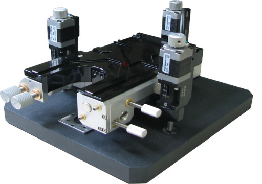
Scanning Probe & Metrology Systems
High-resolution surface characterization and in-situ manipulation tools for nanoscale research and process control.
- check_circleScanning Probe Microscope — AFM / STM / SNOM
- check_circleNano Indentation System
- check_circleNon Contact Optical Profiler
- check_circleNanopositioning & Nano Measuring Systems
- check_circleIn-situ Capabilities — Nanocleaning, Nanoindentation, TEM Lamella Preparation, IV Characterization, Nanocutting, Nanocladding
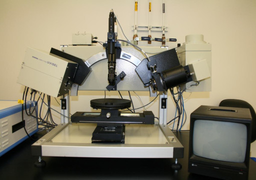
- check_circleSpectroscopic Ellipsometer
Lithography & Pattern Definition
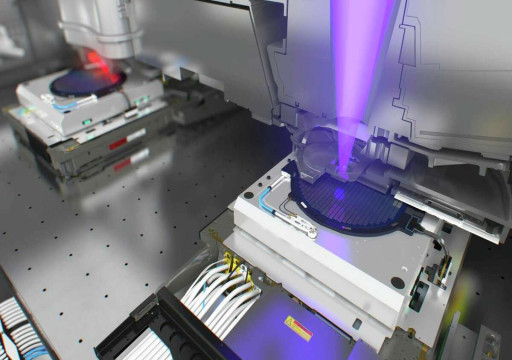
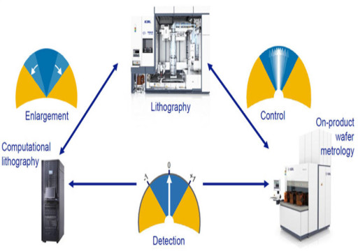
Complete lithography solutions from mask alignment and UV exposure to e-beam writing and nanoimprint for sub-micron patterning.
- check_circleLithography System — Lithography Upgrades for SEMs, Beam Blankers, X-Y Stages for SEM
- check_circleE-Beam Lithography System
- check_circleNano-Imprint
- check_circlePhotolithography — Mask Aligner, Collimated UV Exposure Systems, Spin Coater, Developer, HMDS
- check_circleLaser Pattern Generator
- check_circleVision Based CD Measurement System
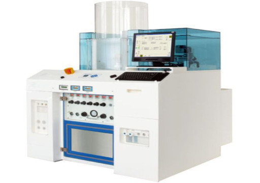
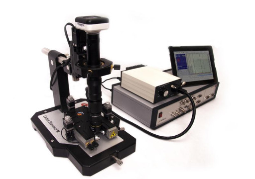
Thin-Film Deposition & CVD
Industry-leading deposition platforms for advanced materials including CNT, Graphene, 2D materials, oxides and nitrides.
- check_circleThermal CVD, LPCVD and PECVD Systems — for CNT, Graphene and 2D Materials
- check_circleAtomic Layer Deposition (ALD) System
- check_circlePECVD, ICP PECVD, ECR/Microwave Systems
- check_circleHV/UHV DC/RF Magnetron Sputtering Systems
- check_circleE-Beam & Thermal Evaporation
- check_circleUHV Deposition & MBE System — for Oxides and Nitrides
- check_circleRapid Thermal Annealing System
Etch, Diffusion & Wet Process Systems
Full-process wet and dry etch capabilities alongside diffusion, oxidation and cleaning systems for complete device fabrication.
- check_circleHorizontal & Vertical Diffusion Systems — Oxidation, Atmospheric and LPCVD Process Systems
- check_circleWet Process Stations — Spin Rinser Dryers, Spray Solvent Tool, Spray Acid Tool
- check_circleRIE, ICP-RIE System — Deep Silicon Etch
- check_circlePlasma & Rapid Thermal Annealing System
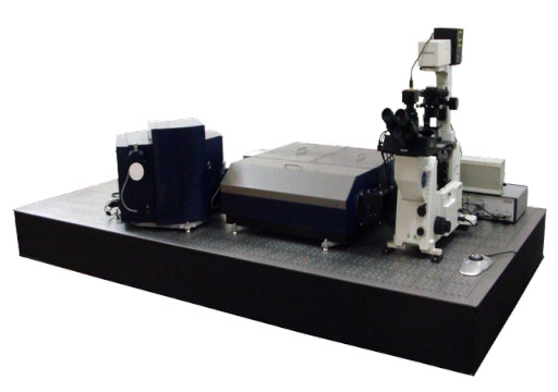
Metrology, Defect Detection & Photovoltaic Instrumentation
Comprehensive inspection, measurement and photovoltaic testing systems for process control and device characterization.
- check_circleAutomated Defect Detection System
- check_circleOptical Stylus System — BOW & WARP Metrology
- check_circleNon Contact Optical Surface Profiler
- check_circleHall Effect Measurement System
- check_circleLED Tester & Probe Station — Manual, Semiautomatic and Fully Automatic
- check_circlePhotovoltaic Instrumentation — Spectral Response/QE Measurement System, Small Area Solar Simulator, Solar Cell I-V Tester, I-V Curve Data Acquisition, Solar Cell Sorter, Spectro Radiometer
Premium instruments from our exclusive brand partners — representing the world's leading manufacturers in nanoscale measurement and analysis.

Atomic Force Microscope (AFM)
High-resolution nanoscale imaging, force spectroscopy and surface characterisation across research disciplines.
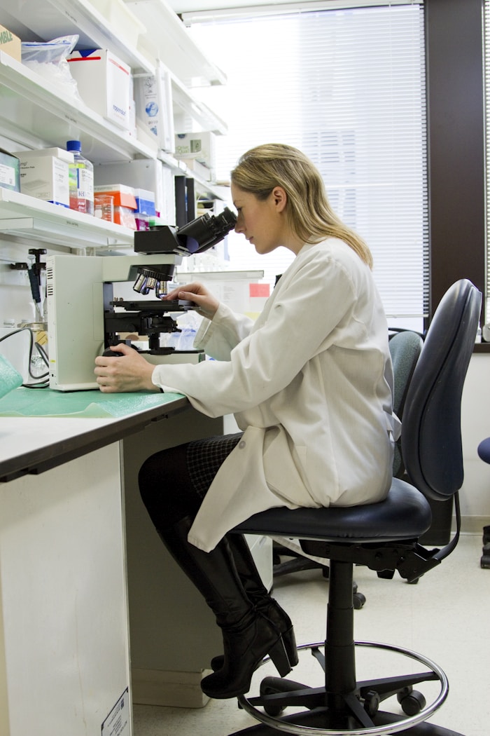
Confocal Raman Microscope
Research-grade confocal Raman system for fast, accurate chemical and structural characterisation.

PIV Flow Measurement System
Non-intrusive full-field velocity measurement for fluid mechanics and aerodynamics research.

Imaging Spectroscopic Ellipsometer
Combines ellipsometry and microscopy for thin film characterisation and microanalysis across multiple fields.

Bench-top Raman Analyser
Compact bench-top system for routine quality control, materials identification and composition analysis.
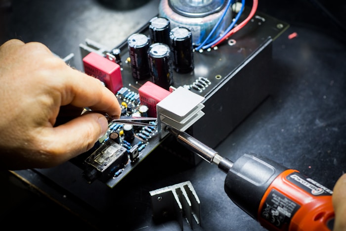
Digital Image Correlation (DIC)
Full-field 2D/3D strain and deformation measurement for materials testing and structural mechanics.
Ready to Equip Your Nanotechnology Lab?
Contact our team for a full equipment list, technical datasheets, pricing and support tailored to your research requirements.